Challenges in Miniaturized Prototype PCB Assembly

Miniaturized Prototype PCB Assembly
The push for smaller, more efficient electronic devices is reshaping the PCB industry. But the trend also poses unique challenges, especially when it comes to prototype PCB assembly. To guarantee the performance and functionality of densely packed components in miniaturized prototypes, precision fabrication, advanced inspection technologies, and cutting-edge testing methods are essential.
Prototypes are a crucial step in the development process for any electronic design. They help verify and refine an original idea, and enable quick error detection and rectification. They also offer an opportunity to test the physical dimensions of a design and determine its fit within a device. As the size of PCBs shrink, prototyping becomes more complicated, with the need for tighter tolerances and precise placement. This requires specialized equipment and a partner with the right expertise.
With miniature components like 01005-size resistors and capacitors, even minor placement inaccuracies can create significant issues like short circuits, poor connectivity, and signal loss. Placement errors can also compromise the quality of solder joints, causing mechanical stress and posing a risk of failure. To ensure high-quality PCB prototypes, manufacturers must implement advanced placement systems that employ a combination of high-precision pneumatic nozzles, servo-motor-driven mechanisms, machine learning, and microscopic optics for pattern recognition. Unfortunately, these solutions often raise costs and slow production.
Miniaturized PCBs are often made with thinner layers and reduced copper weight, resulting in a reduction of available space for transmission lines and components. To address this issue, HDI (high-density interconnect) technology enables designers to fit more components into compact spaces by using thin transmission lines, stack-up layers, and micro-vias. But this solution has its own set of challenges, including ensuring the effectiveness of the circuit’s thermal management solutions.
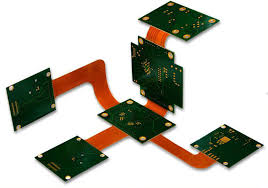
Challenges in Miniaturized Prototype PCB Assembly
Due to their smaller size, miniaturized PCBs have less surface area to disperse heat. Combined with higher component density, this can lead to excessive heat buildup and reduce the life of the circuit board. To combat this, manufacturers must use innovative designs and materials to increase the efficiency of heat dissipation and protect the reliability of miniaturized PCBs.
The heightened proximity of components in miniaturized PCBs can also cause crosstalk and other interference between signal lines, requiring meticulous strategic positioning of parts and traces. This process, called design for manufacturability, is a critical aspect of creating successful miniature prototypes.
The key to overcoming the unique challenges in miniaturized prototype printed circuit board assembly is partnering with an experienced manufacturer with the right tools and skills. This can include utilizing assembly automation and high-precision robotics to ensure the consistency and accuracy of repeated tasks, and optimizing assembly processes based on production volume, environmental conditions, and the specific components used.
An experienced manufacturer can also offer a range of assembly services, from assembling fine-pitch integrated circuits and small packages (01002, BGAs, flip chips) to mounting leadless devices. To ensure the best results, choose a provider that offers comprehensive prototyping and fast production times.