How Are Micro Vias Tested For Reliability?

Micro Vias
The success of high-density interconnect (HDI) designs depends on the strength and reliability of microvia interconnections. But how are micro vias tested for reliability? In this article, we discuss the process of testing stacked and staggered microvias using interconnect stress test (IST) methods. We also identify a number of factors that can impact the performance of microvias and offer a few key design tips.
Microvias are used in PCBs to facilitate solder bridging between adjacent traces. During the solder reflow process, the molten solder flows into the gap between the PCB pad and microvia body to form a solid connection. Despite the small size of these structures, the resulting solder joints are surprisingly strong and can survive many reflow cycles. Nevertheless, it is important to follow the DFM guidelines for microvias and avoid gaps between solder mask and pads.
A common failure mode for stacked microvias is the separation of the micro vias body from the PCB pad due to high tensile stress during the reflow soldering process. This can result in shorts between the pad and trace. This is more common for complex stacked microvia structures, with stack heights above two. However, this separation does not seem to be related to the geometry of the microvia body, but rather the severity of the end-use application environment.
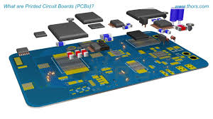
How Are Micro Vias Tested For Reliability?
The number of reflow cycles needed for the failure of multi-level stacked and staggered microvias depends on a variety of factors, including the pitch and spacing of the vias. When the microvias are closely spaced, they can effectively resist expansion and reduce mechanical crosstalk between them. In addition, the close proximity of the microvias increases their structural strength by acting like rivets to hold down the area, enhancing reliability.
During IST tests, the microvias are subjected to mechanical and electrical testing. The results are analyzed to identify trends in the data. Initially, the electrical testing results were relatively flat and did not correlate with either the microvia diameter or pitch. Upon further analysis, the data showed that a correlation did exist between the microvia diameter and the via-to-via distance. This result is a reminder that a successful layered PCB design must include the proper microvia geometries for both electrical and thermal performance.
In the past, it was not uncommon to design a layered PCB with microvias without evaluating their thermal properties and/or construction. This led to difficult-to-detect failures post-assembly. However, the current trend is to use a D coupon for both electrical and thermal stress testing. The D coupons are designed to contain different propagated via structures and transitions in order to accurately test and predict PCB assembly defects. The D coupons can be fabricated with both stacked and staggered vias to ensure they are capable of surviving the various testing processes including DC current induced thermal cycle test, microvia thermal shock testing and IPC-TM-650 2.6.27.