
How Are Solder Joints Inspected For Quality in Flex Circuit Manufacturers?

Solder Joints Inspected For Quality in Flex Circuit Manufacturers
As a flex circuit manufacturer, you have to make sure that your PCB has flawless solder joints. This is a crucial step in the manufacturing process, and can have a huge impact on quality and reliability. To ensure this, you must use the right inspection method. Visual inspection is an effective tool for detecting defects, but it can be labor-intensive and inaccurate. Using machine learning techniques, however, can improve this process significantly. Using this technology, you can automatically inspect the PCB for solder joint defects in a fraction of the time and with much greater accuracy.
Traditionally, visual inspection was carried out by human eyes. This is an expensive, labor-intensive, and error-prone process that can lead to inaccuracies. Modern automated optical inspection (AOI) systems are designed to detect defects that can be missed by humans, such as poor-quality solder joints and polarity mismatches. These systems have become the dominant force in the flex circuit manufacturing industry, mainly because they can offer faster and more comprehensive inspection than traditional methods.
There are several different types of flex circuit manufacturer inspection technologies, including AOI, x-ray, and cross-sectioning. AOI inspects populated PCBs for assembly flaws, such as shorts, opens, and impedance. It also checks for layer registration and identifies missing components.
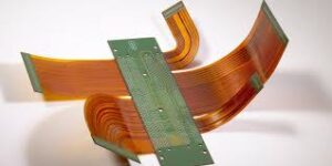
How Are Solder Joints Inspected For Quality in Flex Circuit Manufacturers?
The underlying technology behind AOI is feature-to-model matching. This method identifies features in an image by comparing them to a predefined model. The model is trained by feeding a large dataset of defective and non-defective images. Then, it uses these examples to learn to recognize patterns and anomalies that indicate defects. Once the model has learned these patterns, it can automatically detect defects in new data. This allows AOI to achieve higher levels of accuracy than manual inspection and saves significant amounts of labor.
In order to accurately determine the location of solder joints in a PCB, it is necessary to identify all the standard features that represent the soldering point. To do this, a new solder joint information segmentation method is developed, which employs a multistage image processing pipeline. First, the color image is histogram-equalised to guarantee that all the pixels have the same distribution of hue gamut data. Then, the image is converted to the H (hue) layer and binarised.
The resulting feature map is used as input to the discriminant model. This model aims to distinguish solder joints from the background, which is achieved by increasing the solder joint information segmentation threshold by a factor of 10. Finally, the resulting image is obtained. The model is then tested for the ability to correctly identify solder joints. It is found that the new method outperforms the existing Selective Search and Select Joint methods in terms of identifying the correct position of each soldering point. Moreover, it is more accurate than the other two methods in terms of the size of each soldering point. In addition, the new method is more efficient than the previous ones in terms of resource usage and model generalisation capabilities.

