
How is testing done during PCB manufacturing?

testing done during PCB manufacturing
Testing is a critical component of the PCB (Printed Circuit Board) manufacturing process, ensuring that the final product meets the required specifications and performs reliably in its intended application. As electronic devices become increasingly complex, the importance of thorough testing has grown significantly. Effective testing strategies help identify defects early in the manufacturing process, reduce the risk of product failures, and improve overall quality. This article explores the various methods of testing conducted during pcb manufacturing.
Before manufacturing begins, Design Verification Testing (DVT) is carried out to validate the PCB design. This phase involves using simulation tools to ensure that the design meets the necessary electrical and mechanical specifications. DVT helps identify potential issues such as signal integrity problems, thermal issues, and layout concerns that could affect performance. By addressing these issues at the design stage, manufacturers can reduce the likelihood of costly revisions and rework later in the production process.
Once the PCBs are manufactured, Automated Optical Inspection (AOI) is one of the first testing methods employed. AOI systems use high-resolution cameras to visually inspect the surface of the PCBs for defects such as misaligned components, soldering issues, and physical damage. The images captured are compared to a predefined reference image of the ideal PCB, allowing for the quick identification of defects. AOI is a highly efficient method that can detect issues early in the production process, significantly reducing the risk of defective boards reaching the assembly line.
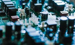
How is testing done during PCB manufacturing?
In-Circuit Testing (ICT) is performed after the PCB has been assembled with components. This method involves using a bed-of-nails test fixture that makes contact with test points on the PCB to verify the functionality of individual components and their connections. ICT checks for issues such as shorts, opens, and incorrect values, ensuring that each component functions as intended. This form of testing is highly effective in identifying defects that may not be visible through visual inspection alone and is commonly used for high-volume production runs.
Functional testing is a comprehensive method used to assess the overall performance of the assembled PCB. This testing checks whether the PCB operates according to its specified functional requirements. Functional tests can include powering up the device, applying specific signals, and monitoring the outputs to ensure they meet the expected results. This method provides a thorough evaluation of the PCB’s functionality and is essential for products that require strict performance standards.
Burn-in testing is a reliability test designed to identify early failures in PCBs. During this test, the assembled boards are subjected to elevated temperatures and voltages for an extended period, simulating real-world operating conditions. The purpose of burn-in testing is to stress the components and detect any weaknesses that may lead to failures during normal operation. This proactive approach helps ensure that only reliable PCBs are delivered to customers.
Environmental testing assesses how well the PCB can withstand various environmental conditions, such as temperature fluctuations, humidity, and exposure to chemicals. This type of testing is especially important for PCBs used in harsh environments, such as automotive and industrial applications. Tests may include thermal cycling, humidity exposure, and salt spray tests to evaluate the board’s durability and long-term performance.
After all testing phases are complete, a final quality control inspection is conducted. This step ensures that the PCB meets all specified requirements and standards before it is shipped to customers. Quality control may include a final visual inspection, checking for compliance with industry standards, and reviewing documentation to confirm that all testing processes were properly followed.
In conclusion, testing during PCB manufacturing is a multi-faceted process that plays a vital role in ensuring the quality and reliability of the final product. From design verification to final quality control inspection, each testing method addresses specific aspects of the PCB’s performance and functionality. By implementing rigorous testing protocols, manufacturers can minimize defects, enhance product reliability, and ultimately deliver high-quality PCBs that meet the demands of the ever-evolving electronics market.

